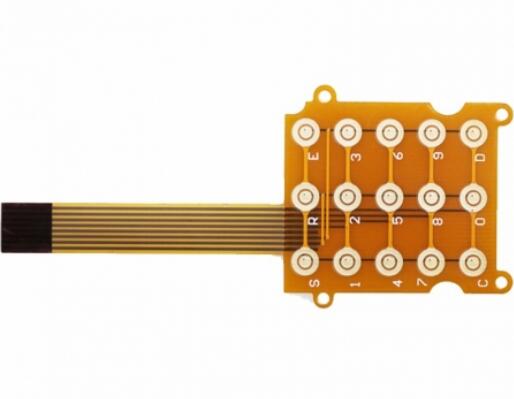
Due to the many processes of FPC soft board, it brings a little difficulty to the production control, resulting in some product defects. The common defects of FPC board surface include bubbles, resistance welding in holes, skip printing, also known as flying white, oxidation, patterns with pinholes, dirt on the surface, uneven surface, double shadow, inconsistent colors on both sides and cracks, etc. The following is a detailed description according to the actual situation of the factory.
1. Bubbles appear between lines or after the side development of a single line
Main reasons: Bubbles between two or more lines are mainly caused by too narrow line spacing and too high lines. During screen printing, the solder block cannot be printed on the substrate, resulting in the presence of air or moisture between the solder block and the substrate. During curing and exposure, the expansion of the gas caused by heat is mainly caused by the high lines. When the scraper contacts with the line, the line is too high, and the angle between the scraper and the line increases, The solder mask cannot be printed to the root of the line, so that there is gas between the side of the line root and the solder mask layer, and bubbles will be generated after heating.
Solution: During screen printing, visually check whether the screen printing material is completely printed on the substrate and line side wall, and strictly control the current during electroplating.
2. There are solder resistances and pinholes in the hole
Main reasons: FPC FPC FPC FPC FPC FPC FPC FPC FPC FPC FPC FPC FPC FPC FPC FPC FPC FPC FPC FPC FPC FPC FPC FPC FPC FPC FPC FPC FPC FPC FPC FPC FPC FPC FPC FPC FPC FPC FPC FPC FPC FPC FPC FPC FPC FPC FPC FPC FPC FPC FPC FP. There is dirt on the photographic plate, which causes the FPC FPC FPC FPC FPC FPC FPC FPC FPC FPC FPC FPC FPC FPC FPC FPC FPC FPC FPC FPC FPC FPC FPC FPC FPC FPC FPC FPC FPC FPC FPC FPC FPC FPC FPC FPC.
Solution: print paper in time and select high-mesh screen for plate making; Always check the cleanliness of the photographic plate during exposure.
3. There are signs of blackening on the copper foil line under the solder mask
Main reasons: FPC FPC FPC FPC FPC FPC FPC FPC FPC FPC FPC FPC FPC FPC FPC FPC FPC FPC FPC FPC FPC FPC FPC FPC FPC FPC FPC FPC FPC FPC FPC FPC FPC FPC FPC FPC FPC FPC FPC FPC FPC.
Solution: Visually check the copper foil on both sides of the printed board for oxidation during screen printing.
4. Dirt and uneven surface
Main reason: the dirt on the surface is caused by flying hairs and other sundries in the air, and the uneven surface is caused by not paying attention to printing paper in time and removing the residual ink of the screen plate during screen printing, resulting in uneven surface.
Solution: The cleanliness of operators should be fully guaranteed in the clean room to avoid irrelevant personnel walking through the clean room, clean the clean room regularly, and print paper in time to remove the residual ink of screen printing.
5. Doubling and cracking
Main reason: ghost is because the FPC flexible circuit board is not firmly positioned during screen printing and the residual ink on the screen plate is not removed and accumulated on the printed board in time, resulting in regular ink spots around the entire FPC pad. Cracking is due to insufficient exposure during FPC exposure, resulting in small cracks on the board surface.
Solution: fix firmly with positioning pins and print paper in time to remove residual ink on the screen; The exposure measurement makes the comprehensive value of the exposure lamp energy, exposure time and other parameters reach 9-11 exposure levels, and there will be no cracking in this range.
6. Inconsistency of color on both sides and skip printing flying white
The main reason is that the number of knives for screen printing on both sides is very different, and there is also the mixing of new and old ink. It is possible that one side is the new ink that has been stirred, and the other side is the old ink that has been used for a long time.
Skip printing is caused by excessive electroplating current and thick coating, resulting in too high graphic lines. When screen printing FPC flexible circuit boards, because the scraper knife and screen printing frame are at a certain angle for screen printing, the line on both sides of the line is too high, and the ink will not be placed, causing skip printing. Another reason is that the scraper knife has a gap, and the gap does not place ink, resulting in skip printing.
Solution: Try to keep the same number of knives for screen printing and avoid mixing new and old ink; Mainly control the electroplating current and check whether there is a gap in the scraper blade.

Online
Service
ConsultationTime:9:00-18:00
Hot
Line
0755-27847787
7*24H Service
Follow
Us
 Website